
TOPCon vs HJT vs Perovskite-Silicon Tandem Cells: Efficiency & LCOE Analysis
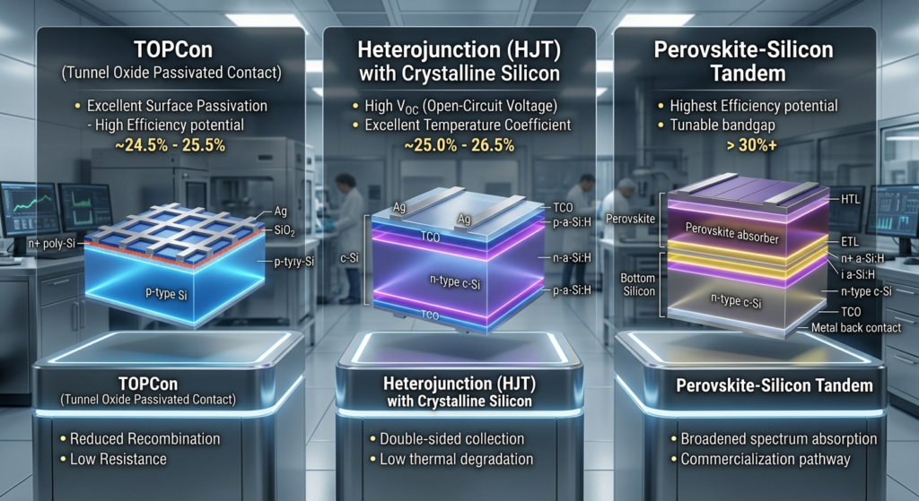
Table of Contents
- 1. Executive Summary: The Post-PERC Photovoltaic Paradigm Shift
- 2. Thermodynamic Fundamentals & The Shockley-Queisser Limit
- 3. Architectural Deep Dive: N-Type TOPCon Technology
- 4. Architectural Deep Dive: Silicon Heterojunction (HJT) Technology
- 5. The Next Frontier: Perovskite-Silicon Tandem Photovoltaics
- 6. Comparative Engineering Analysis: TOPCon vs HJT vs Perovskite-Silicon Tandem Cells
- 7. Degradation Dynamics & Temperature Coefficient Physics
- 8. Manufacturing CAPEX, OPEX, and Levelized Cost of Electricity (LCOE)
- 9. Strategic Utility Roadmap (2026–2035)
- Technical References & Academic Citations
The global solar sector is undergoing its most aggressive technological transition in years. The last comparable shift was the commercial replacement of p-type Aluminum Back Surface Field (Al-BSF) cells by Passivated Emitter and Rear Cell (PERC) architecture. PERC is reaching its practical efficiency ceiling of approximately 24.5%. Utility-scale developers, EPC firms, and module manufacturers are pivoting in response. They are moving toward advanced n-type silicon architectures and multi-junction device physics. Evaluating TOPCon vs HJT vs Perovskite-Silicon Tandem Cells is now the primary strategic directive for maximizing energy yield and lowering the Levelized Cost of Electricity (LCOE).
N-type Tunnel Oxide Passivated Contact (TOPCon) and Silicon Heterojunction (HJT) cells are mature, highly scalable silicon-wafer technologies. Comprehensive TOPCon vs HJT vs Perovskite-Silicon Tandem Cells benchmarks show something different for multi-junction architectures. Those break through the theoretical limitations of single-junction silicon entirely. This technical analysis evaluates TOPCon vs HJT vs Perovskite-Silicon Tandem Cells across utility and commercial deployment profiles. It covers semiconductor physics and recombination thermodynamics. It covers manufacturing steps, temperature coefficients, and degradation mechanisms. It also covers the techno-economic factors.
Understanding the core operational differences in TOPCon vs HJT vs Perovskite-Silicon Tandem Cells is essential for photovoltaic engineers, energy project developers, and system designers. By examining quantum efficiency, charge carrier transport, and thermal coefficient dynamics, this study establishes clear operational benchmarks for next-generation solar installations.
1. Executive Summary: The Post-PERC Photovoltaic Paradigm Shift
For over a decade, p-type monocrystalline PERC dominated commercial solar manufacturing due to low production costs and compatible tooling. However, p-type silicon suffers from inherent material limitations—most notably Light-Induced Degradation (LID) caused by boron-oxygen complexes. In contrast, n-type silicon wafers are doped with phosphorus, eliminating boron-oxygen LID entirely and offering superior resistance to metallic impurities, which yields higher minority carrier lifetimes.
The market transition in TOPCon vs HJT vs Perovskite-Silicon Tandem Cells is defined by distinct technological imperatives:
- TOPCon (Tunnel Oxide Passivated Contact): Serves as the immediate successor to PERC. It uses an ultra-thin tunnel oxide layer of about 1.5 nm. That is paired with a heavily doped polycrystalline silicon layer. The combination achieves ultra-low surface recombination velocities. It also preserves up to 70 to 80% of existing PERC cell production lines.
- HJT (Silicon Heterojunction): Combines the advantages of crystalline silicon (c-Si) with thin amorphous silicon (a-Si:H) passivating layers. HJT features a completely symmetrical cell architecture, high bifaciality rates (>85–90%), and exceptional performance in hot climates due to an industry-leading temperature coefficient.
- Perovskite-Silicon Tandems: Represents a multi-junction paradigm. Tandem devices layer a high-bandgap metal halide perovskite top cell, at about 1.68 eV, directly over a low-bandgap silicon bottom cell at about 1.12 eV. Each layer captures a different region of the solar spectrum. That minimizes thermalization losses.
2. Thermodynamic Fundamentals & The Shockley-Queisser Limit
The fundamental theoretical efficiency ceiling for single-junction solar cells exposed to unconcentrated AM1.5G solar radiation is dictated by the Shockley-Queisser (S-Q) Limit. Take a crystalline silicon cell with a bandgap of 1.12 eV. Its maximum theoretical power conversion efficiency is approximately 29.4%. That figure accounts for intrinsic Auger recombination.
Thermalization vs. Non-Absorption Losses
Single-junction photovoltaic devices are inherently constrained by two primary thermodynamic loss mechanisms:
- Non-Absorption Losses: Photons with energy ($h\nu$) below the semiconductor bandgap ($h\nu < E_g$) pass through the absorber layer without exciting an electron-hole pair.
- Thermalization Losses: Photons with energy significantly higher than the bandgap ($h\nu > E_g$) excite charge carriers high into the conduction band. The excess energy ($h\nu – E_g$) is rapidly lost as heat via phonon emission as the carrier relaxes back to the conduction band edge.
In analyzing TOPCon vs HJT vs Perovskite-Silicon Tandem Cells, single-junction single-absorber materials inevitably lose over 50% of incoming solar irradiance to thermalization and non-absorption. The theoretical efficiency ceiling of single-junction architectures is defined by the following expression for maximum extractable power density ($P_{max}$):
Pmax = q * Voc * Jsc * FF = ∫ E * Φ(E) * η(E) dE
In this equation, $q$ is elemental charge and $V_{oc}$ is open-circuit voltage. $J_{sc}$ is short-circuit current density and $FF$ is fill factor. $\Phi(E)$ is photon flux density. $\eta(E)$ represents external quantum efficiency as a function of energy. Evaluating TOPCon vs HJT vs Perovskite-Silicon Tandem Cells shows how tandem cells overcome the single-junction S-Q limit. They stack two absorbers with complementary bandgaps. That raises the theoretical thermodynamic limit for a double-junction system to ~45%.

3. Architectural Deep Dive: N-Type TOPCon Technology
TOPCon cell architecture relies on passivated contact technology to minimize minority carrier recombination at the metal-semiconductor interface—the primary area of efficiency loss in standard PERC cells.
Passivated Contact Mechanism
A standard TOPCon cell features a thin tunnel silicon oxide (SiO2) layer with a thickness of 1.2 to 1.6 nanometers grown on the rear surface of an n-type silicon substrate, followed by a thin layer of heavily doped n+ polycrystalline silicon (poly-Si). The physics governing this system includes:
- Quantum Mechanical Tunneling: The SiO2 layer is thin enough to allow majority carriers (electrons) to tunnel through quantum-mechanically with minimal resistance.
- Chemical Passivation: The tunnel oxide saturates dangling bonds at the crystalline silicon surface, drastically reducing surface state density ($D_{it}$).
- Field-Effect Passivation: The high concentration of phosphorus dopants in the poly-Si layer induces an electric field that repels minority carriers (holes) away from the contact interface.
This design allows TOPCon cells to achieve Open-Circuit Voltages ($V_{oc}$) exceeding 730–735 mV in mass production, compared to 685–695 mV for high-efficiency PERC cells. Evaluating TOPCon vs HJT vs Perovskite-Silicon Tandem Cells highlights TOPCon’s primary advantage: manufacturing compatibility. Existing PERC lines can be upgraded to TOPCon by adding Chemical Vapor Deposition (LPCVD/PECVD) equipment for poly-Si deposition and tunneling oxide growth.
4. Architectural Deep Dive: Silicon Heterojunction (HJT) Technology
Silicon Heterojunction cells replace traditional diffused p-n junctions. They use low-temperature amorphous silicon thin films instead. Those films are deposited on both sides of an n-type monocrystalline silicon wafer.
Bandgap Engineering & Symmetrical Structure
The core innovation of HJT is the integration of high-bandgap amorphous silicon (~1.7 eV) with low-bandgap crystalline silicon (1.12 eV). A high-efficiency HJT cell consists of the following layers:
- N-Type c-Si Wafer Core: Absorbs infrared and visible light, providing high carrier lifetimes (>10 ms).
- Intrinsic Amorphous Silicon (i-a-Si:H): Ultra-thin (~5 nm) intrinsic layers deposited on both front and rear surfaces to provide near-perfect chemical passivation of c-Si surface states.
- Doped Amorphous Silicon Layers: A p-doped a-Si:H layer on the front forms the emitter junction. An n-doped a-Si:H layer on the rear forms the Back Surface Field.
- Transparent Conductive Oxide (TCO): Layers deposited over the amorphous silicon layers to collect current, as amorphous silicon exhibits poor lateral conductivity.
Because amorphous silicon passivates surface states effectively, HJT cells routinely achieve production $V_{oc}$ values of 745–755 mV. The front and rear cell layer stacks are symmetrical. That gives HJT cells a natural bifaciality factor of 85% to 95%. It significantly outperforms TOPCon at 75 to 85% and PERC at 70%. In comprehensive TOPCon vs HJT vs Perovskite-Silicon Tandem Cells market assessments, HJT stands out as an optimal substrate for tandem deposition. Its flat surface topology and high $V_{oc}$ are the reasons.
5. The Next Frontier: Perovskite-Silicon Tandem Photovoltaics
To transcend the 29.4% S-Q threshold, researchers and manufacturers are stacking metal halide perovskites directly onto bottom silicon cells. Metal halide perovskites feature the general crystal formula ABX3 (where A = Cs, Methylammonium [MA], Formamidinium [FA]; B = Pb, Sn; X = Cl, Br, I).
Monolithic (2-Terminal) vs. Mechanically Stacked (4-Terminal) Architectures
Perovskite-silicon tandem cells are primarily constructed in two configurations:
- 4-Terminal (4T) Tandems: The perovskite top cell and silicon bottom cell are manufactured independently and coupled optically. While electrically isolated (eliminating current-matching requirements), 4T designs require additional transparent conductive substrates and extraction electronics, increasing balance-of-system (BOS) costs.
- 2-Terminal (2T) Monolithic Tandems: The perovskite top cell is deposited directly onto the silicon bottom cell connected by a Recombination Layer / Interconnecting Layer (ICL). 2T tandems require fewer manufacturing materials, lower BOS costs, and offer higher practical efficiency potential (>33–35%), though they mandate strict current-matching between top and bottom cells.
In a 2T monolithic structure, the top perovskite layer absorbs high-energy ultraviolet and visible photons. Its bandgap is about 1.68 eV. Low-energy near-infrared photons pass through instead. The bottom silicon cell absorbs those, at a bandgap of about 1.12 eV. Direct side-by-side studies of TOPCon vs HJT vs Perovskite-Silicon Tandem Cells confirm one point clearly. 2T monolithic tandems offer the highest theoretical efficiency potential of any commercially scalable technology.
6. Comparative Engineering Analysis: TOPCon vs HJT vs Perovskite-Silicon Tandem Cells
A comprehensive side-by-side technical evaluation highlights the physical, structural, and performance metrics across all three technologies.
| Engineering Parameter | N-Type TOPCon | Silicon Heterojunction (HJT) | Perovskite-Silicon (2T Tandem) |
|---|---|---|---|
| Lab Cell Peak Efficiency | 26.8% | 27.3% | 34.6% |
| Commercial Module Efficiency | 22.5% – 23.5% | 23.0% – 24.2% | 26.0% – 28.5% (Pilot 2026) |
| Open-Circuit Voltage (Voc) | 730 – 738 mV | 745 – 755 mV | 1,800 – 1,920 mV |
| Bifaciality Factor | 75% – 85% | 85% – 95% | 65% – 80% |
| Temperature Coefficient | -0.30% / °C | -0.26% / °C | -0.20% to -0.24% / °C |
| Manufacturing Complexity | Moderate (12–13 steps) | Low Process Steps (8 steps) | High (Multi-layer vacuum/solution) |
| CAPEX per GW ($ Nominal) | $25M – $30M (PERC Upgradeable) | $40M – $50M (New Lines) | $65M – $80M (Early Stage) |
| Degradation Year 1 / Annual | 1.0% / 0.40% per year | 0.8% / 0.35% per year | 2.0% / 0.80% per year (Uncertified) |
Analyzing TOPCon vs HJT vs Perovskite-Silicon Tandem Cells yields three conclusions. TOPCon holds a short-term cost advantage. HJT offers superior long-term performance metrics. Tandems deliver unprecedented power density per square meter.
7. Degradation Dynamics & Temperature Coefficient Physics
Solar modules operate in field environments subject to high temperatures, moisture ingress, and thermal cycling. Mechanical stability and long-term degradation dictate bankability for non-recourse project financing.
Temperature Coefficient Impact on Energy Yield
Solar cell temperature rises above standard test conditions of 25°C in real deployment. Semiconductor bandgaps narrow as it does. Open-circuit voltage then drops, according to the material’s temperature coefficient. Operating power output ($P(T)$) as a function of cell temperature ($T$) is defined as:
P(T) = PSTC * [ 1 + γ * (T – 25°C) ]
When operating in high-irradiance regions where field cell temperatures reach 65°C ($T – 25 = 40^\circ\text{C}$):
- TOPCon (γ = -0.30%/°C): Incurs a power loss of $40 \times -0.30\% = \mathbf{-12.0\%}$.
- HJT (γ = -0.26%/°C): Incurs a power loss of $40 \times -0.26\% = \mathbf{-10.4\%}$.
This difference yields a 1.6% relative yield gain for HJT over TOPCon in hot climate environments, offsetting initial CAPEX premiums.
Degradation Mechanisms: PID, LeTID, and Perovskite Instability
Comparative field longevity reveals unique failure modes across each architecture:
- Potential-Induced Degradation (PID): High system voltages (1500V DC) cause sodium ion drift toward the cell surface. TOPCon requires robust front-passivation encapsulation (such as POE film) to mitigate PID symptoms.
- Light and Elevated Temperature-Induced Degradation (LeTID): Affects certain silicon formulations due to hydrogen state transitions. HJT is largely immune to LeTID due to low-temperature processing (<200°C).
- Perovskite Degradation Triggers: Perovskites break down when exposed to moisture, oxygen, ultraviolet radiation, and heat above 85°C. Those conditions cause phase transformations. Photoactive perovskite structures convert into non-photoactive yellow phases ($PbI_2$). Resolving halide segregation via Advanced Atomic Layer Deposition (ALD) encapsulation is essential for commercial scaling.
8. Manufacturing CAPEX, OPEX, and Levelized Cost of Electricity (LCOE)
Evaluating TOPCon vs HJT vs Perovskite-Silicon Tandem Cells requires examining total lifecycle financial models. The Levelized Cost of Electricity (LCOE) incorporates total capital expenditures, fixed operational maintenance (O&M), and lifelong generation yield:
LCOE = [ CAPEX + ∑ (OPEXt / (1 + r)t) ] / ∑ (Energy Generationt / (1 + r)t)
Manufacturing Economics Overview
- TOPCon CAPEX Efficiency: TOPCon benefits from existing PERC manufacturing infrastructure. Adding LPCVD/PECVD tooling costs ~$5M–$8M per GW, keeping total line costs low (~$25M–$30M/GW). Silver paste consumption remains a cost challenge, requiring dual-side screen printing.
- HJT Capital Requirements: HJT requires specialized plasma-enhanced chemical vapor deposition (PECVD) and physical vapor deposition (PVD) equipment, increasing greenfield CAPEX to ~$40M–$50M/GW. However, HJT reduces silver consumption by utilizing low-temperature silver-coated copper pastes, lowering processing thermal budgets.
- Tandem Cost Reduction Curves: 2T tandems deliver up to 20 to 30% higher power output per square meter. Balance-of-system costs fall proportionally on a per-watt basis as a result. Those costs include tracker steel, land acquisition, cabling, and installation labor. The result is lower overall LCOE.
9. Strategic Utility Roadmap (2026–2035)
The transition dynamics within the global solar market point to a phased deployment trajectory across all three cell architectures:
- Phase 1 (2026 to 2028), TOPCon Market Dominance: TOPCon will lead mainstream solar manufacturing. It should capture over 65% of global market share. Low production costs and legacy PERC conversions drive that.
- Phase 2 (2028 to 2032), HJT Expansion and Early Tandem Pilots: HJT will expand its share in utility-scale projects in high-temperature environments. It will also serve as the primary commercial bottom-cell substrate for 2T perovskite tandem pilot lines.
- Phase 3 (2032 to 2035 and beyond), Commercial Perovskite Tandem Scale: Accelerated encapsulation testing must first prove 25-year outdoor durability. Once it does, monolithic perovskite-silicon tandem modules will redefine premium efficiency standards. They should capture high-value residential, commercial, and land-constrained utility segments.
Analyzing TOPCon vs HJT vs Perovskite-Silicon Tandem Cells confirms that solar technology development is moving steadily toward multi-junction physics. TOPCon provides immediate scale, HJT offers optimized temperature performance and bifaciality, and Perovskite Tandems pave the way toward efficiency levels beyond 30%.
Technical References & Academic Citations
- Explore renewable energy technologies and photovoltaic engineering analyses at SolarSunLabs.
- Review zero-carbon transportation and energy research at ZeroCarbonDrive.
- Access health metrics and biomedical technology analyses at SymptomDesk.
- Examine research on high-efficiency silicon photovoltaics at the National Renewable Energy Laboratory (NREL).
- Track international solar PV technological progress via the International Energy Agency (IEA).
- Review solar manufacturing standards and technical guidelines at the International Organization for Standardization (ISO).
- Analyze solar cell efficiency tables and device physics research in Nature Energy.
Our tandem solar cells guide works through the details.
Related Posts


Leave a Comment
Your comment will be published after it has been approved. Please send comments that do not contain slang words.